Spectral characterization of PIC devices is key to test accuracy
Previsouly published in PIC Magazine
Author: François Couny
March 2020
p. 22 - 24

The challenge of testing complex photonic integrated circuits (PICs) remains a key requirement to speed production while improving device reliability and the quality of finished products. EXFO describes key issues and solutions for improved testing of passive PIC components.
BY F. COUNY, PHD, EXFO PRODUCT LINE MANAGER
AS DISCUSSED RECENTLY in the article TAP into the power of PIC (PIC Magazine Issue 4, 2019), one of the key challenges to unlocking the full potential of photonic integrated circuits (PICs) is the test, assembly and packaging (TAP) aspect. This is not only because the process is slow and expensive, but also because component characterization is at the heart of the PIC development chain, helping improve design, foundry wafer production and final testing after packaging. Although tried-and-tested optical measurement techniques exist for fiber-based components, the sheer volume and complexity of new PIC devices create a new paradigm where testing speed and measurement reliability requirements are taken to a whole new level. In this article, we will discuss optical spectral characterization techniques that can take on those new challenges.
Optical testing – Now a critical consideration
Testing electronic integrated circuits has two main advantages over photonic testing:
- The manufacturing process leverages 60+ years of continuous improvement
- Only a few, easily accessible, electronic test points of known functionalities are needed on the chip to ensure excellent chip-to-chip homogeneity throughout the wafer
PIC fabrication processes have dramatically improved over the past 10 years, particularly thanks to specialized foundries (both for Silicon Photonics and for Indium Phosphide) and thanks to PIC component measurement databases made available through process design kits (PDK). Even though the industry has taken big leaps to improve manufacturability, photonic integrated circuit fabrication is still maturing. Homogeneity of the PIC chips, over even a small wafer, still requires individual component testing. This explains why many test points are required for the full characterization of key functionalities on the chip. Overall, today’s testing of the individual building block is critical even as new test results help improve design and fabrication.
Testing the building block – What to look for?
Thanks to the advent of the transceiver in telecom applications, testing active optical components such as lasers or semiconductor optical amplifiers (SOA) is somewhat easier than testing passive optical devices. For the former, an optical spectrum analyzer (OSA) is often sufficient for spectral characterization, whereas for the latter, passive components transform light by filtering, actively or passively switching, or simply guiding light through what seems to be endless combinations of optical building blocks, providing complex spectral features that need to be accurately measured.
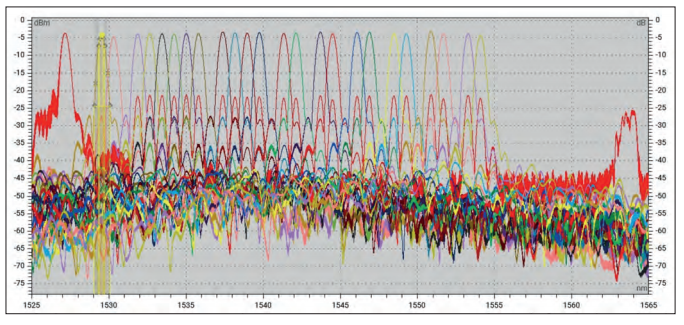
The key parameter when testing passive optical components is the insertion loss, i.e., the amount of light lost when going through a device. This is particularly important in telecom optical devices. PIC based interferometric systems such as ring resonators or Mach-Zehnder modulators can achieve extremely high Q-factor leading to spectral features (peaks or troughs) that are only a few picometer in width. Hence, these devices require high resolution spectral characterization of the insertion loss. Spectral testing in different configurations (e.g. applied voltage in the case of modulators) then provides information about the usable wavelength range, their free spectral range or expected extinction ratio.
Reducing test time while boosting measurement reliability will lower operational expenses in PIC development. Full automation and seamless integration of the optical test solution into the characterization setup can help achieve this. Ideally, a single piece of optical test equipment should perform several tasks within a photonics test setup, including fiber to chip alignment (this also keeps capital expenditures under control). Bearing in mind that since PICs can operate over a large spectral range, photonic chip manufacturers should look for flexible and scalable solutions to address various wavelength ranges.
OSA to the rescue
The first part of any PIC spectral characterization is coupling light in and/or out of the optical chip. To do so requires a fast photodiode and alignment algorithm to quickly reach maximum coupling.
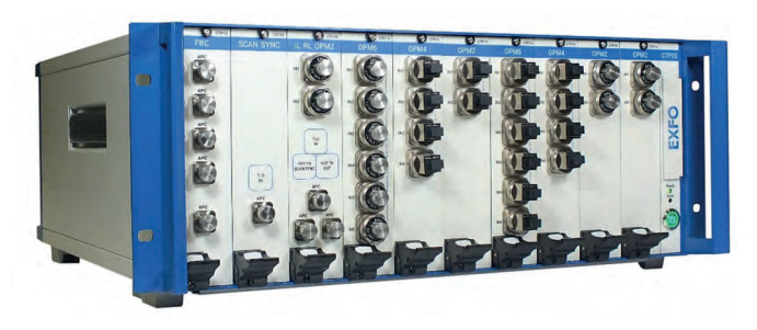
Although a simple laser and photodiode would suffice to perform this alignment, the real payoff is in using a component tester, such as the CTP10 from EXFO, which provides real-time photodiode measurements in addition to high-quality spectral measurements.
Once best alignment is achieved, some further configurations may be required on the PIC device itself (e.g. set up of voltage on a modulator).
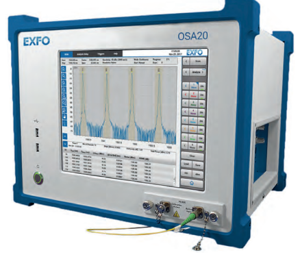
In that case, a possible test setup would make use of a superluminescent LED (SLED) or an amplified spontaneous emission (ASE) light source in conjunction with a fast optical spectrum analyzer (OSA), like the OSA20 from EXFO. Such an OSA can provide real-time spectral information several times per second, a refresh rate that is fast enough for optimizing the PIC under test. However, this method has two key limitations:
- OSAs typically only have a single input, meaning only one optical port can be tested at a time
- Due to the spectral bandwidth of the monochromator (the optical filter inside the OSA), picometer-resolution spectral measurement is not possible. Nonetheless, the OSA technique can be used for components with low loss and limited spectra contrast, where spectral features are of the nanometer order.
Leveraging the highest resolution
To facilitate insertion loss measurements of components with complex, high contrast spectral features, the most efficient and reliable setup is the swept laser technique. This method uses a continuously tunable laser to scan the wavelength across the spectral range of interest. Operating synchronously with the laser, a component tester (like EXFO’s modular component test platform CTP10) is then used to record the optical power of each output port of the device under test.
The use of tunable lasers to perform such a test has several obvious advantages over the broadband source and OSA method:
- Insertion loss measurement can be performed with picometer resolution because of the intrinsic narrow linewidth of the laser (significantly below 0.1 pm)
- The high power of the laser source also allows testing of several hundred output ports simultaneously and with good dynamic range (typically over 70 dB)
- The fast-tuning speed of the laser allows characterization within a few seconds.
However, such high measurement specifications can only be achieved with a state-of-the-art component tester yielding short test times and excellent accuracy. The instrument dynamically and simultaneously records the test wavelength and output power as the laser is being swept. New test and measurement instruments such as the CTP10 tap into the latest advances in optics and detection technologies to measure – in a couple of seconds – the insertion loss of high-port count devices with 1-pm resolution.
A larger spectral range (important when characterizing components operating over extended spectral ranges) can also be tested using several tunable lasers, each covering a portion of the total spectrum under test and concatenating the insertion loss result into a single spectrum. On the CTP10, this is achieved simply by adding a full-band combiner (FBC) module to the system.
Future-proof it
Innovative solutions are being designed to help PIC manufacturers overcome the testing bottleneck. A final word of advice is to choose solutions that can scale and adapt to tomorrow’s challenges as well.
Flexibility will be key as the demand for passive optical components and their use become ever so critical in shaping the future.