Signal Conditioning of 100 GigE Electrical Lanes
Now that 40G/100G systems have become a reality, key transceiver vendors are working hard to provide optical CFP modules that require specific signal conditioning of their electrical interfaces in order to operate properly. For CFP-based optical modules, the various 40G/100G configurations available today involve transmitting multiple optical channels in either WDM over SMF, or parallel optics run individually on parallel MMF ribbon fiber. For instance, in the case of 40G transmission, the optical signal is sent in a 4 x 10G configuration, while for 100G transmission, it is sent in a 4 x 25G or 10 x 10G configuration. In either case, the optical signal is derived inside the CFP module from individual 10.3 Gbit/s electrical lanes at the module interface, namely the CAUI or XLAUI interface. Each of the 10.3 Gbit/s CAUI lanes must be analyzed and optimized electrically to achieve the best possible performance and minimize errors that can be caused by any signal integrity issue on this interface.
High-Speed Signal Integrity Issues
PCB materials, electronic devices, connectors, components and trace lengths implemented in a signal interface will exhibit signal-distortion characteristics that will be specific to that interface and the optics that are used. The following examines the critical issues that can affect the integrity of high-speed signals.
PCB Materials
High-speed signals need to travel a path with minimum loss and with the various materials used today, FR-4 (fiberglass-based plastic laminates) can affect signal quality. FR-4 is mostly chosen for its low cost, its availability and its generally good performance, but with the current high-speed interfaces—10 Gbit/s and beyond—permittivity, loss coefficient and other material properties gain importance in terms of attenuation and distortion, and can very easily compromise signal quality, as well as the integrity of the interface.
An alternative to compensating for such signal degradations is to use different materials that have relatively lower loss coefficient and permittivity. However, these types of materials are generally more expensive and are only used where absolutely required, whereas FR-4 is much more commonly deployed, especially for backplanes and a majority of board designs.
Most of the signal degradation can be easily observed through the effects of jitter in the signal. These effects can be seen more clearly when separating the various jitter components and observing them on an oscilloscope. In short, the total jitter is namely comprised of data-dependent jitter (DDJ), one type of DDJ being inter-symbol interference (ISI). ISI can help detect a drop in signal quality due to loss in the media induced by the transmitted data pattern.
Transmitting a pattern such as 101010101010 through a specific path at a high enough speed using FR-4, followed by an eye-diagram test performed at the far end, will probably result in a compromised eye diagram, as seen in Figure 1. The fast transitions, delay and loss in the media will prevent the signal from getting to a full “1” or “0” level. By replacing the data pattern with one that has less transitions (such as 111100001111), signals have more time to reach their respective “1” and “0” levels, resulting in a far better eye opening.
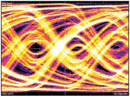
Figure 1. Typical example of a compromised high-speed signal.
Electronic Compensation
As mentioned previously, the component selection and placement, the connectors, as well as the trace length, also contribute to signal degradation and distortion, making it sometimes impossible to compensate for by only choosing better PCB materials. Other solutions must then be considered, such as signal pre-emphasis, de-emphasis and equalization, to aid in compensating for signal loss/reflection in the transmission path of various high-speed interfaces.
Pre-Emphasis
The use of pre-emphasis, which essentially pre-distorts or modifies the energy/frequency content of signal transitions (see Figure 2), compensates for signal degradation by effectively reducing reflections and crosstalk, while improving ISI. It is key to apply a known level of energy or pre-distortion on the transition or bits, to help minimize high-frequency effects and allow the signal to reach its destination at the receiver with improved detection ability, such as represented by the eye diagram shown in Figure 3.
Pre-emphasis can be set with multiple taps—a tap being the coefficient that will be added to the corrected bit. A one-, two- or three-tap selection can be used to determine the right amplitude to be applied to the corrected bit. A similar analysis can be conducted for post- or de-emphasis where the correction will be applied to the post-bits.
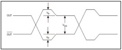
Figure 2. Theoretical example of applying pre-emphasis on a digital signal.
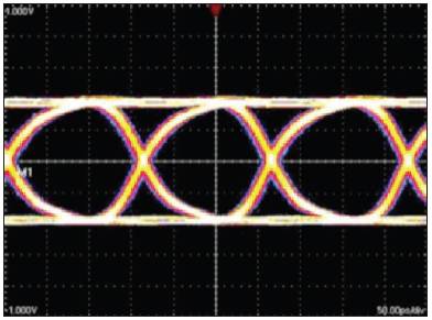
Figure 3. Example of pre-emphasis improving the eye diagram at the receiver.
Equalization
Since emphasis is mostly used at the transmitter, the receiver’s detection capabilities can be enhanced through equalization. This process offsets the high-frequency effects of the transmission path by applying the reverse transfer function of the frequency-energy content of the signal compromised by the transmission path. Non-linear amplification of the degraded frequency components in the signal is applied in an amount that is inversely proportional to the loss or distortion in which the components were affected by the signal transmission medium. This improves the imaginary eye opening that would be seen inside the chip after the equalization circuit, as represented by the imaginary eye diagrams of Figures 4a and 4b.
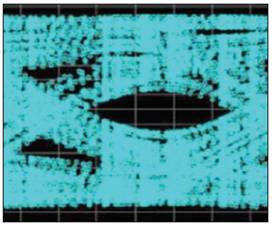
Figure 4a. Representative of an equalized signal inside a receiver.
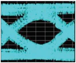
Figure 4b. Representative example of an equalized signal inside a receiver.
CAUI and XLAUI Signal Analysis
EXFO was the first on the market to offer a signal-conditioning tool on its FTB-85100G Packet Blazer 100G/40G Ethernet Test Module. This feature helps characterize and troubleshoot electrical-level issues on standard optical interfaces used within 100G/40G systems. In fact, it allows direct access to amplitude and pre-/post-emphasis control of the 10G electrical CAUI/XLAUI lane transmitters (see Figure 5), as well as equalization correction at the receivers.
The signal-conditioning interface provides access to the electrical parameters, enabling the user to better compensate for signal-integrity issues or modify specific electrical parameters to observe the effects of stressing the pluggable optical device. Having the ability to modify signal parameters with a wide dynamic range of amplitude, pre-emphasis and equalization controls allows CFP manufacturers to evaluate and optimize the performance of their modules.
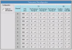
Figure 5. Control panel for CAUI/XLAUI interface.
Conclusion
With today’s links integrating more and more high-speed devices and the resulting need to optimize and characterize high-speed signals and interfaces, relying on network/component test equipment featuring a built-in signal-conditioning tool delivers clear benefits to technicians, engineers, network installers and optical component manufacturers. It provides them with a much easier, much more flexible way to identify issues, validate the design of their components, and ultimately optimize network performance.

