TAP into the power of PIC

Previously published on PIC Magazine
P. 44
Author: François Couny, Subject Matter Expert
December 2019
Photonic integrated circuits (PICs) promise dramatic size, power and efficiency advances compared to legacy bulk optical modules and CMOS electronics. The rapid roll-out of PICs has been hindered by slowly developing automated test, assembly and packaging technologies due to the complexities and variabilities common to PICs. The experts at EXFO share insights into ways that TAP needs are now being met.
PHOTONIC INTEGRATED CIRCUITS (PICs) are a well-known technology in the telecom world, mainly thanks to the frantic development of transceivers and passive components that are smaller, faster, cheaper and greener than their bulk-optics counterparts. PICs are also getting traction–both from a commercial and research perspective - in other sectors, too: lab-on-achip, LIDAR technology and quantum computing are but a few applications were PICs are of great benefit.
The move towards PICs at an accelerated rate is made possible by production techniques that allow more components to be fit onto a single, highperformance chip, cutting down on cost, size and power consumption. This is strikingly similar to what happened with electronic ICs some 40 years ago. A single PIC chip today can already contain thousands of components, each of them with multiple inputs and outputs.
Test, assembly and packaging (TAP) is, in this context, often referred to as ‘the bottleneck,’ i.e., the last hurdle to fully unleash the power of PICs. Whilst TAP is fully optimized for the electronic IC, it is still in its infancy when it comes to photonics—taking a large chunk of the cost-per-chip (around 80%). Photonics has some stringent limitations due to the light itself: it is not as easy to manipulate photons as it is to ‘play’ with electrons! Coupling light in and out of a device using optical fiber with a 10 μm core requires expertise. This makes the whole business of testing and packaging PICs more daunting and, as a result, those final processes are left to the end-user. However, those processes now need to be addressed in a way that would allow hundreds of thousands of components to be made every year.
When it comes to testing PIC components, the need for speed comes with new requirements on more stringent specifications. Even more so when considering that data acquired during the testing phase is fed back throughout the various processes comprising PIC development: PIC manufacturers and the foundries can learn about performance tolerances of a particular fabrication process, while PIC design software can be made more accurate by calculating directly what the optical performance of a chip could be based on process design kits (PDKs) provided by the foundries. A new breed of components, not even available in bulk optics, have started to pop up over the past couple of years, making it even more difficult to measure spectral features that are, in some cases, a few picometers wide and exhibit spectral contrast well over 2000 dB/nm.
How do we unlock this photonic conundrum?
The key is to provide a flexible and scalable solution to test every parameter and function on a complex chip in a fast and reliable way. The testing capabilities needed must cover a wide range of things including a mix of optical, electronic and sometimes radio frequency (RF) signals and spans from fundamental measurements such as peak wavelength or optical power for active components (i.e., emitting light), to spectral characteristics such as insertion loss and polarization dependent loss for passive optical components (i.e., transmitting and transforming light), to fully functional characterization such as bit-error rate (BER) or constellation measurement. Consider all the various configurations of the component and you have an idea of the challenge when it comes to testing PICs effectively.
The recipe for success?
A comprehensive approach where the chip is designed to allow fast and reliable testing directly onto the wafer, i.e., before the chips are diced, is a viable solution. Wafer testing allows identification of bad chips and avoids costly packaging of defective devices. Multiple optical test points can be aligned, and light coupled from optical fibers hovering above the surface of the wafer into the chip on the wafer is possible. Using optical fiber arrays or bundles and/or photodiodes to monitor the optical output alleviates the need for repeated single fiber alignment whenever possible. In this context, fast and reliable alignment algorithms operate jointly with automated test equipment to sort out good chips from the bad ones or to provide an optimized test setup that can ‘map’ the characteristics of a wafer and provide feedback to foundries and create PDKs. The value of this automation is that non-specialist personnel can operate the test system with ease.
PIC-specialized wafer probe stations—such as those designed by MPI Corporation—can address the high requirements of testing 200mm or 300mm sized PIC wafers. This includes the seamless integration of the alignment equipment onto the probe station without consuming additional floor space and Sentio® software for convenient operations. Along with the development of the grating coupler, allowing the coupling of light from optical fiber to PIC wafer, those stations have come a long way to address problems specific to PIC devices. Besides the standard usage of electrical probing, the photonic test components also need to be integrated. Therefore, the probe station not only requires good vibration isolation towards the ground floor but also excellent stability of the probe plate where the photonic alignment positioners are placed.
Alignment needs can vary greatly depending on the devices to be tested. They can be as simple as a three-axis stage for single fiber applications where the fiber is aligned using a fiber holder with a predefined angle matching the grating coupler geometry for optimum coupling either in or out of the device. More sophisticated is the integration of a hexapod positioner which comes with three additional axis for rotation of yaw, roll and pitch. This functionality is mandatory for fiber array alignments.
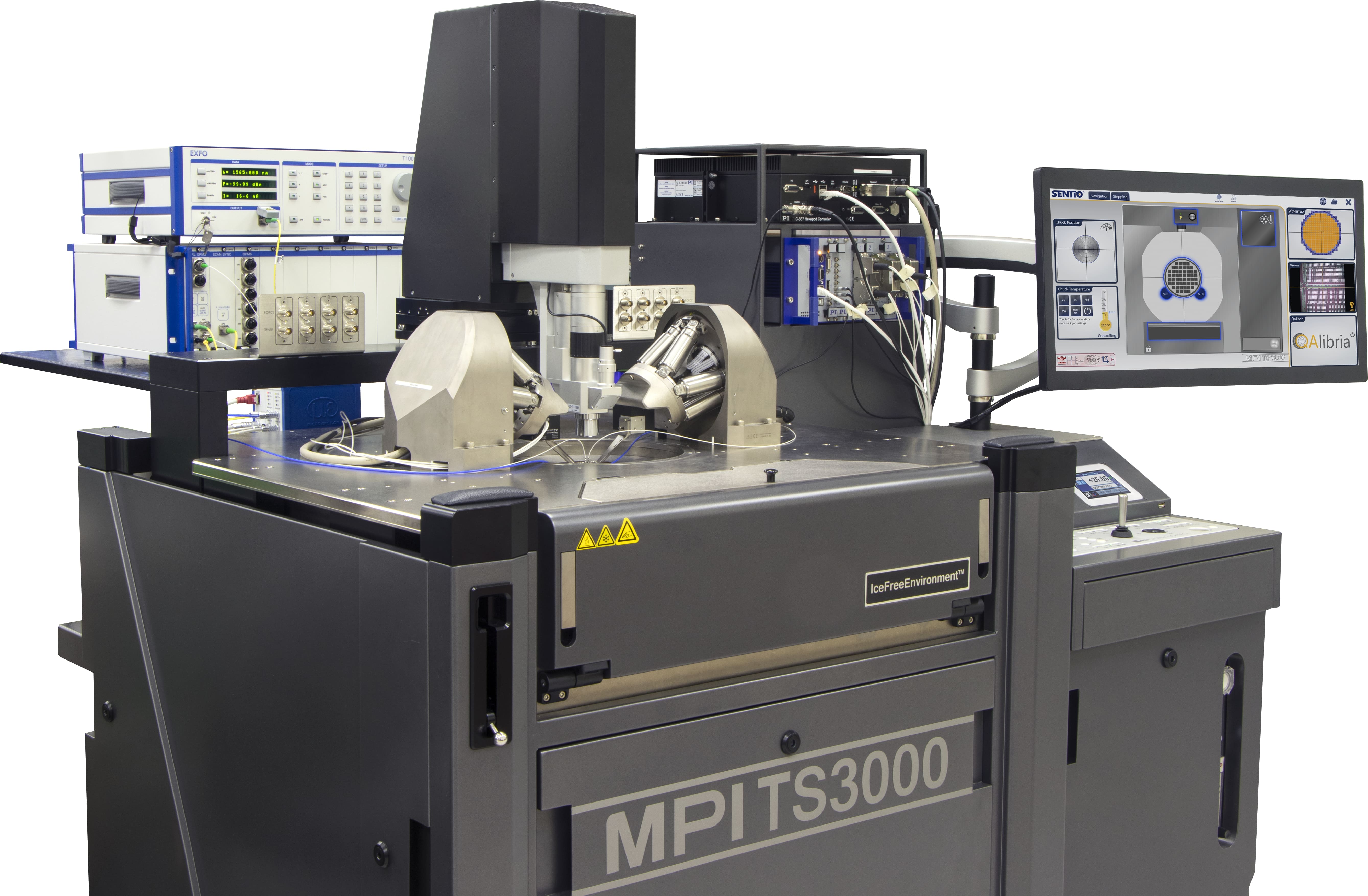
Depending on the device being tested, the station could have one or two optical positioners. This is dependent on whether the test device has just one (Opto-Electric; O-E or Electro-Optic; E-O) or two (Optical-Optical; O-O) optical ports: one-sided devices may be light-emitting devices for instance, where the stimulation is done electrically (E) and the output measured optically (O) or light-detecting devices where the optical input (O) is transformed into an electrical signal (E). Setting up the alignment can be very time-consuming. Because of that, a lot of effort has been put into the automation of alignment procedures. State-of-the-art wafer probe systems can align single fiber devices under one second before taking a measurement. For fiber arrays, automatic alignment is even more critical as any rotational misalignment is automatically corrected. Fragile single fibers can easily cause damage if they are allowed to crash into each other or the wafer. Probe station software nowadays recognize the fiber positions relative to each other and to the wafer to prevent collisions.
It is clear from these developments that ‘designed according to test’ PIC chips are key in reducing testing time while boosting reliability. Symbiosis between design, fabrication and testing is the path to understanding and addressing any issue throughout the PIC development process. The same holistic principle can be applied during PIC assembly and the final packaging of the component to further reduce the impact of TAP on the final chip cost.
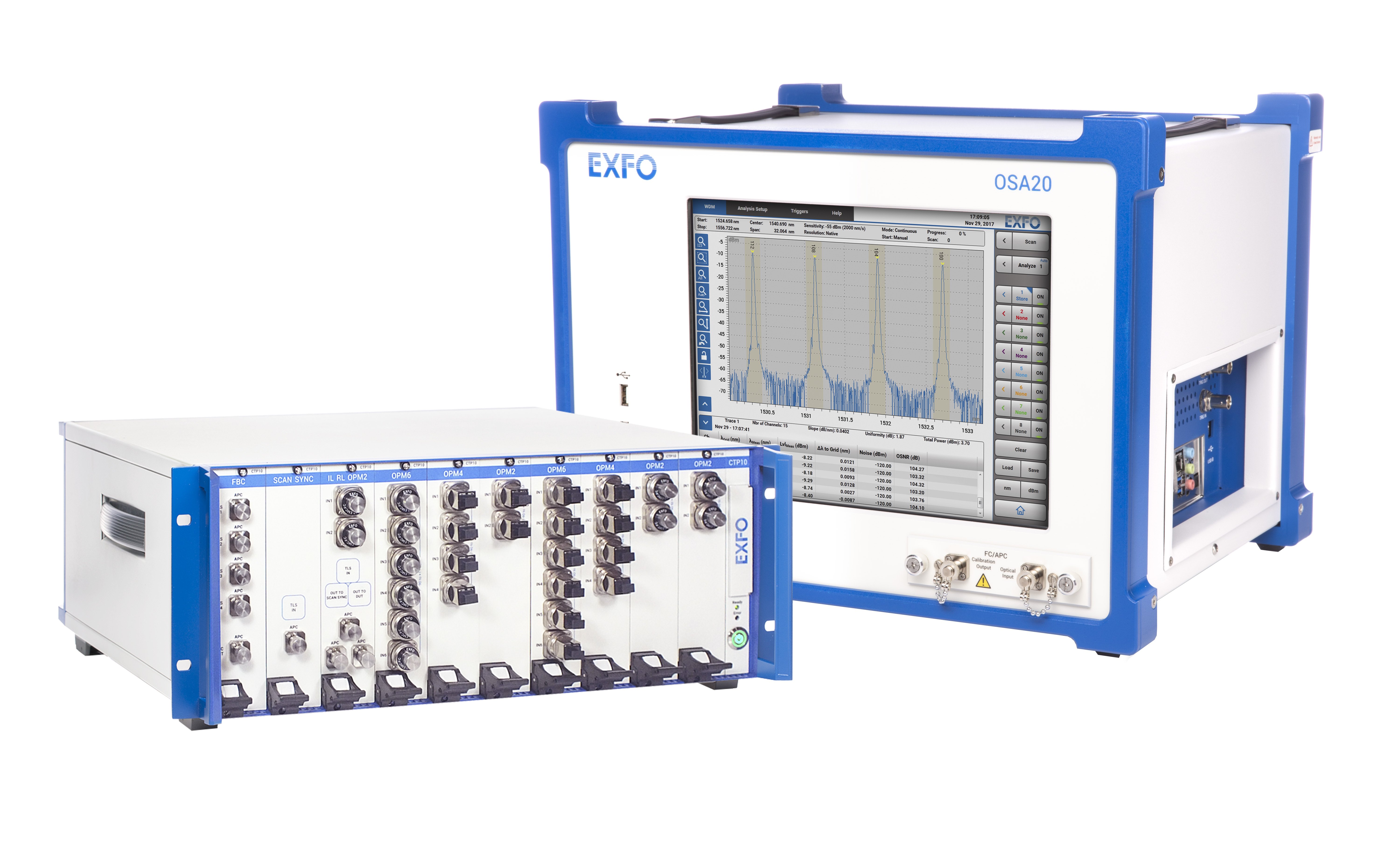
Another important challenge is photonic characterization, which requires speed and reliability at an unprecedented level in the photonics world, in a similar way to advances achieved in electrical testing over past decades. New characterization solutions based on state-of-the-art electronics and opto-mechanics enable accurate spectral measurements in under one second. Those instruments need to be able to measure large spectral contrast with an ever-increasing wavelength accuracy and over a large number of inputs and outputs. Although optical spectrum analyzers (OSA), such as EXFO’s OSA20, provide high-resolution spectra in less than 300 ms for both active (i.e., light-emitting) and passive (i.e., light passes through) components, they are better suited for the former. For the latter, a laser swept technique provides optimal results. Using the CTP10 component testing platform from EXFO, picometer resolution spectral response of tens of output can be simultaneously obtained in a few seconds. Data post-processing time is also reduced thanks to onboard spectra analysis and measurement automation.
By integrating the CTP10 into the MPI probe station environment, it is possible to operate all required functions from just one single platform. Fiber-grating coupler alignment can be performed where the optical coupling signal is converted into a voltage information by the CTP10 to feed into the alignment system. The spectral measurement is then performed by CTP10 software on trigger from the probe station control software. This enables fully automated wafer testing including die-to-die stepping, fiber alignment and measurement.
Conclusion
Matching the maturity of electronic IC testing takes a strong roadmap that has to incorporate standardization testing throughout the PIC development process. This would ensure reliable methods for testing components that can be complex while allowing for the required scaling up to volume manufacturing. This, in turn, allows testing by non-specialist operators with limited training while providing accurate test data to PDKs so that some functionalities or characteristics are obtained ‘by design’ on a wafer: testing a few chips on the wafer could then validate the whole chip set. Finally, standardized optical testing using future-proof solutions is expected to dramatically reduce test time and cost whilst remaining flexible and evolutive.
Acknowledgement
The author acknowledges the valuable contribution of Sebastian Giessmann, Product Marketing Manager for the Advanced Semiconductor Test Division at MPI Corporation.